Ethereum's Memory Hardness Explained

April 28th, 2017 - Vijay Pradeep
As crypto-currencies increase in value, so does the payout from mining them. This creates a substantial economic incentive to not only deploy more mining hardware, but to also develop faster, more efficient mining hardware. We saw this with bitcoin: Mining migrated from CPUs, to GPUs, to FPGAs, and now to ASICs [1]. Today, Ethereum GPU mining is the norm, but the miners haven’t made the jump to running the ethereum mining/hashing algorithm, ethash, on specialized hardware solutions (e.g. FPGAs and ASICs). Plenty of articles and forums attribute this to ethash being memory hard (a.k.a. memory bound). Here, I’ll walk through where Ethereum mining’s memory hardness comes from, and what the next generation of custom ethereum mining hardware might look like. For this article, I’m assuming readers have a general understanding of standard computer technologies and crypto-currency blockchains, but don’t need to be programming or mining experts. For a more technical, programmer-oriented explanation of Ethereum’s mining algorithm, called ethash, please refer to the ethash page on the ethereum wiki. For a less technical introduction to blockchains, visit the blockgeeks blockchain guide here.
Quick Refresher on Proof-of-Work Mining
In proof-of-work mining, miners are tasked with generating a short binary blob (called a nonce), which, when hashed, produces an output value less than a pre-specified target threshold. Due to the cryptographic nature of each currency’s hash function, there is no way to reverse-engineer or back-compute a nonce that satisfies the target threshold limit. Instead, miners must “guess-and-check” hashes as fast as possible, and hope they’re the first miner in the entire crypto-currency’s network to find a valid nonce.
How the Ethereum Ethash Hashing Algorithm Works
The Ethash algorithm relies on a pseudorandom dataset, initialized by the current blockchain length. This is called a DAG, and is regenerated every 30,000 blocks (or every ~5 days). As of March 2017, the DAG was ~2GB [2], and the DAG will continue grow in size as the blockchain grows. The specifics of how to generate the DAG aren’t so relevant for this article, but you can read more about DAG generation in this stack exchange answer.
The flow of the ethash hashing algorithm can be summarized as follows:
The Preprocessed Header (derived from the latest block) and the Current Nonce (the current guess), are combined using a SHA3-like algorithm to create our initial 128 byte mix, called Mix 0 here.
The Mix is used to compute which 128 byte page from the DAG to retrieve, represented by the Get DAG Page block.
The Mix is combined with the retrieved DAG page. This is done using a ethereum-specific mixing function to generate the next mix, called Mix 1 here.
Steps 2 & 3 are repeated 64 times, finally yielding Mix 64.
Mix 64 is post processed, yielding a shorter, 32 byte Mix Digest.
Mix Digest is compared against the predefined 32 byte Target Threshold. If Mix Digest is less than or equal to Target Threshold, then the Current Nonce is considered successful, and will be broadcast to the ethereum network. Otherwise, Current Nonce is considered invalid, and the algorithm is rerun with a different nonce (either by incrementing the current nonce, or picking a new one at random).
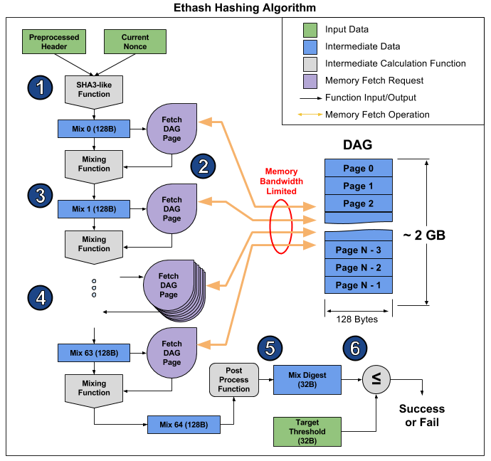
Figure 1 - Algorithmic flow for how Ethereum’s ethash hashing algorithm works (Vijay Pradeep - Source)
Why Is This Memory Hard?
Every mixing operation requires a 128 byte read from the DAG (See Figure 1, Step 2). Hashing a single nonce requires 64 mixes, resulting in (128 Bytes x 64) = 8 KB of memory read. The reads are random access (each 128 byte page is chosen pseudorandomly based on the mixing function), so putting a small chunk of the DAG in an L1 or L2 cache isn’t going to help much, since the next DAG fetch will very likely yield a cache miss. Since fetching the DAG pages from memory is much slower than the mixing computation, we’ll see almost no performance improvement from speeding up the mixing computation. The best way to speed up the ethash hashing algorithm is to speed up the 128 byte DAG page fetches from memory. Thus, we consider the ethash algorithm to be memory hard or memory bound, since the system's memory bandwidth is limiting our performance.
Hitting the Memory Bandwidth Limit in Real Hardware
As an example of how the memory bandwidth limit affects real hardware, let’s take a closer look at the mining performance of a commonly used graphics card: The ATI Radeon RX 470.
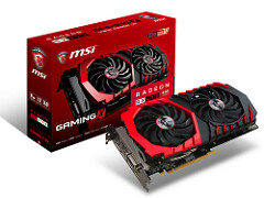
Figure 2 - MSI RX 470 Graphics Card (Source Flikr: CORP Agency)
RX 470 Specs:
Cost: ~$175 (March 2017)
Memory: 8 Gigabytes
Memory Bandwidth: 211 Gigabytes / sec [3]
If the ethash hashing is truly memory hard, we would expect that the actual hashrate for this hardware to be very close to the maximum theoretical hashrate, assuming fetching DAG pages is the only step performed. We can calculate this maximum theoretical hashrate as follows:
(Memory Bandwidth) / ( DAG memory fetched per hash) = Max Theoreticical Hashrate
(211 Gigabytes / sec) / (8 kilobytes / hash) = 26.375 Megahashes/sec or 37.9 nanoseconds/hash.
The empircal hashrate of the RX 470 during real operation is ~24 Megahashes/sec [4], or 41.7 nanoseconds/hash. This is only 3.8 nanoseconds slower than the best possible theoretical hash time calculated above. This small delay can easily be explained by memory latency or other fast operations in the system. Thus, the performance of this graphics card is as expected, assuming that ethash hashing is memory hard and fetching DAG pages is the rate limiting step.
Beating The Graphics Cards: The Road to Custom Ethereum Mining Hardware
The only way custom ethereum mining hardware will make sense is if it is more cost effective or power efficient in memory bandwidth (lower $ / (GB/sec) or lower Watts / (GB/sec)).
Option 1: Design a High Memory Bandwidth FPGA/ASIC Board
Looking at the RX 470, we can do some quick math ($175 / (211 GB/s) ) to see that it costs $0.82 per GB/s. Compared to a single GDDR5 chip (e.g. Micron EDW4032BABG), which costs $6.83 and has a bandwidth of 24 GB/s, we can do better at $0.28 per GB/s. So, if we can build custom chip (either ASIC or FPGA) than can interface with 9 GDDR5 chips, we’ll have a memory bandwidth of 216 GB/s at a price of $61.47. This still isn’t a finished mining product, since we need a FPGA or ASIC memory controller, circuit board, & support electronics. If the shipped final assembly (adding additional parts, processes, testing, & logistics) costs less than the RX 470 (only $175), then the custom board will beat the GPU based card. That is, until a faster, more efficient, cheaper graphics card comes to market. For instance HBM graphics cards cards are already available. But, if you find low cost, off-the-shelf, FPGA or ASIC chips with 5-10 DDR or HBM memory controllers, or your company is experienced in building custom high memory bandwidth ASIC solutions, you may be able to beat out off-the-shelf hardware. But, if in this situation, you should probably change your business model and build graphics cards instead, since that’s already a huge market.
Option 2: Use Next-Gen Mobile Chipsets
As the need for mobile computer vision and advanced mobile 3D graphics grows, we’ll see more mobile-friendly, high memory bandwidth. These include could be mobile system-on-a-chip solutions with an integrated GPU (e.g. NVidia Tegra X1), or a standalone mobile GPU (e.g. PowerVR Series 8XE), or dedicated high bandwidth vision or neural net focused processors with integrated memory (e.g. Movidius Myriad 2). These device classes will continue to evolve, and if the cost, power, & memory bandwidth hit the right sweet spot, we could very possibly see custom ethereum miners with 10-20 mobile GPUs or VPUs arrayed on a single mining board.
Conclusion
The sequential, DAG page fetches in the ethash hashing mining algorithm hits the memory bandwidth limits of modern day hardware, limiting their theoretical maximum hashrate. Will we be seeing custom ethereum miners? Maybe. But when this happens, they probably won’t be ASIC or FPGA based. They’ll likely still be based on off-the-shelf chips (mobile GPUs or VPUs), and not in the traditional graphics card form factor we’re so used to seeing in modern computers.
One Final Caveat: Casper
This article is based on the current Proof-of-Work based ethash protocol being used for for Ethereum mining. In Proof-of-Work based systems such as this, miners perform significant amounts of computation to process new blockhain blocks, and the miners, in return, receive currency rewards. Once the ethereum network transitions to a Proof-of-Stake system, the currency rewards are given to ethereum currency holders instead of miners, likely making ethereum mining obsolete. It’s still unclear when this transition will happen, but you can read more about the Casper transition on the Ethereum blog.
References
[1] - Bitcoin Wiki: Mining
[2] - Ethereum Epoch 111 was 2004874624 bytes, as seen in the C++ ethash code on github here.
[3] - Wikipedia: AMD Radeon 400 Series
[4] - Cryptocompare: Radeon RX 470 Ethereum Mining Stats
[Title Photo] - "Bitcoin mining" - Photo Credit: Marko Ahtisaari, Flickr - License: Attribution 2.0 Generic (CC BY 2.0) - Modified (Cropped Vertically)